What the team built
Researchers at the University of Hong Kong's Department of Electrical and Computer Engineering, with the Center for Advanced Semiconductors and Integrated Circuits (CASIC), have built a gallium oxide (Ga₂O₃) power module that switches 1,000 volts and 1,000 amperes. The work was led by professor Yuhao Zhang, Dr Hehe Gong and PhD student Xin Yang, with professor Guo-Quan Lu of Virginia Tech and professor Jiandong Ye of Nanjing University, and is published in Nature Communications.
Gallium oxide is an ultra-wide bandgap (UWBG) semiconductor. According to the paper, discrete UWBG devices with power-switching capacities up to the kilowatt level had been demonstrated before this work, but a packaged, multi-die UWBG power module had not. The team reports that its module advances the power capacity of UWBG electronics by over two orders of magnitude.
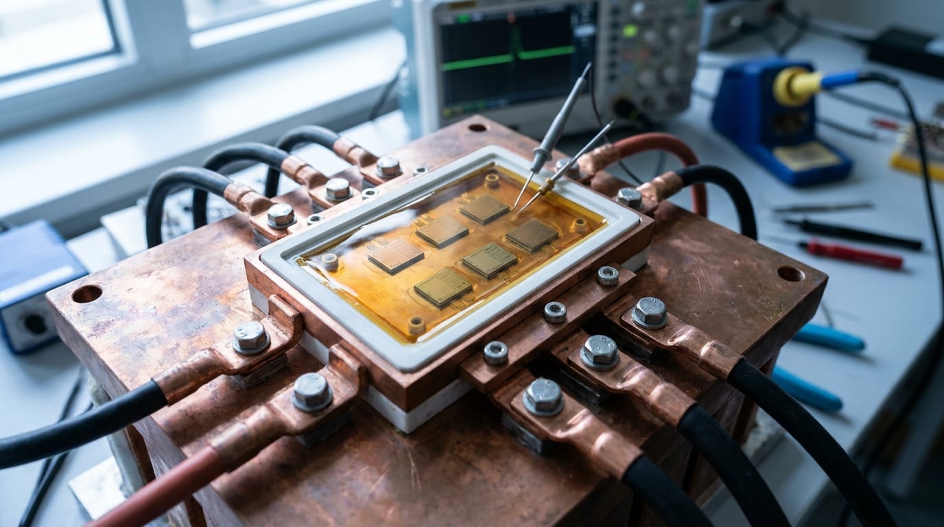
The module is flip-chip packaged and contains six Ga₂O₃ devices. The researchers demonstrated repetitive switching at 1,000 V and 1,000 A at a frequency of 1 kHz, which they state corresponds to a peak power level of one megawatt.
Why gallium oxide is hard to package
The press release states that practical Ga₂O₃ devices have historically been limited to relatively low power for two reasons: the material does not conduct heat efficiently, and packaging multiple devices together becomes increasingly difficult at high voltage and current.
The paper describes the challenge in terms of high electric fields and transient power surges. Its approach is a high-permittivity interface design that allows the device and the package to be optimised together for both electrical and thermal behaviour. The release calls this device-package co-design, in which the electrical field, heat flow and mechanical stress are managed as one system.
How the cooling and field control work
The team introduced a "junction-side cooling" architecture, which places the heat-generating region of the semiconductor close to the cooling path. It also added a high-permittivity insulating layer that helps redistribute the electric field around the device. According to the release, the two measures together let heat escape more efficiently while improving the module's voltage-handling capability.
The paper states that this optimisation maximises the module's transient thermal performance. It allows the high volumetric heat capacity of gallium oxide, described in the paper as a largely untapped advantage in prior device development, to be fully exploited, together with the material's high-temperature stability.
What the tests measured
A single packaged Ga₂O₃ device conducted 234 amperes at 1,000 volts during pulsed operation and remained functional at junction temperatures exceeding 250 °C, according to the release. The six-device module then switched repeatedly at 1,000 V and 1,000 A at 1 kHz.
The paper reports a pulsed power capacity density of over 1.8 MW/cm² for the optimised module, which it says outperforms silicon and wide-bandgap semiconductor counterparts. It also describes fast switching with minimal reverse recovery.
Where the researchers see it being used
The release names pulsed-power applications, where very large amounts of electrical energy must be delivered within microseconds, as particularly promising. It states that pulsed-power systems can take advantage of gallium oxide's volumetric heat capacity to withstand high electric fields and high transient temperatures.
Potential applications listed are high-voltage protection for future power grids, advanced medical systems, particle accelerators and fusion-energy facilities. The release also states that the module's fast switching could enable smaller and more efficient power-conversion systems.
Gong is quoted in the release saying the result provides a scalable approach for translating UWBG material properties into practical high-power systems.
Technical fact box
- 1,000 V and 1,000 A: repetitive switching demonstrated by the six-chip module
- 1 kHz: switching frequency during the demonstration
- 1 MW: peak power level corresponding to that switching, per the researchers
- 234 A at 1,000 V: pulsed conduction of a single packaged Ga₂O₃ device
- Over 250 °C: junction temperature at which the single device remained functional
- Over 1.8 MW/cm²: pulsed power capacity density of the optimised module
- Over two orders of magnitude: increase in UWBG power capacity claimed over previous demonstrations
- Six: number of Ga₂O₃ devices integrated in the flip-chip packaged module
Sources
- A megawatt ultra-wide bandgap semiconductor module for pulsed power electronics — Nature Communications — Hehe Gong, Xin Yang, Boyan Wang et al.
- Engineers develop the world's first megawatt ultra-wide bandgap semiconductor module — Phys.org (Technology)
Discussion
Technical questions and corrections are welcome. Comments are signed and checked before they appear.
No comments yet.
Sign in to add a typed review comment. Reviews are signed with your name.