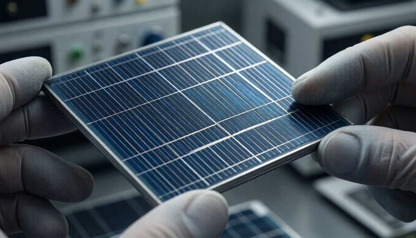
A research group led by Chinese polysilicon and solar module manufacturer Tongwei has built a tunnel oxide passivated contact (TOPCon) solar cell with a selective emitter formed by a non-destructive photoresist-based etching process, pv magazine reports. The work is described in Solar Energy Materials and Solar Cells, with authors from the School of Optoelectronic Science and Engineering at the University of Electronic Science and Technology of China and Chinese industrial equipment company Jiangsu Inspiray Equipment Co., Ltd.
Conventional TOPCon cells face a trade-off between low contact resistance and reduced carrier recombination in the boron-doped emitter, the researchers report. Their architecture combines heavily boron-doped regions beneath the metal contacts with lightly doped regions between them. The non-contacted regions reach a sheet resistance of 1,600 Ω/sq, which corresponding author Xiajie Meng told pv magazine is, to the team's knowledge, the highest reported for TOPCon to date — a claim the article reports rather than an independently verified record.
The team compared a conventional uniform emitter, a boron-doped selective emitter and a locally boron-doped finger structure. The selective emitter combined 450 Ω/sq beneath the metal contacts with 1,600 Ω/sq in non-contacted regions. According to the researchers, this raised average cell efficiency from 25.82% to 25.98%, an absolute improvement of 0.16 percentage points, while open-circuit voltage rose from 742.6 mV to 745.5 mV and fill factor from 83.54% to 83.76%.
The analysis found that increasing sheet resistance in non-contacted regions from 800 Ω/sq to 2,000 Ω/sq improved minority carrier lifetime and surface passivation, but gains became marginal beyond 1,600 Ω/sq and doping uniformity deteriorated, making that value preferable for fabrication. The locally boron-doped finger structure improved passivation but suffered greater fill factor losses, reaching 83.34% against 83.76% for the selective emitter, partly reflecting increased series resistance and potentially additional recombination. Simulations using the Quokka3 simulation software indicated that a contacted-region width of approximately 200 µm gave the highest efficiency among the configurations investigated, and that reducing metal finger widths to 7 µm to 9 µm could allow a denser grid with a pitch of around 500 µm to 550 µm.
Meng stated that for the locally boron-doped finger architecture, simulations suggest higher bulk resistivity wafers with more closely spaced front contacts could offer further improvements, although experimental validation is still required. Meng concluded that the findings could help manufacturers refine emitter doping profiles and contact designs, paving the way for further efficiency gains and potential industrial adoption.
Key facts
- 26.03% certified efficiency of the optimised selective emitter cell, confirmed by ISFH
- 1,600 Ω/sq sheet resistance in non-contacted emitter regions
- 0.16 percentage points absolute average efficiency gain over a uniform emitter (25.82% to 25.98%)
- 746.5 mV open-circuit voltage of the optimised cell
- 450 Ω/sq sheet resistance beneath the metal contacts
Sources
- Tongwei unveils 26.03%-efficient TOPCon solar cell with high sheet resistance — pv magazine
Other news outlets are named as sources but not linked.
Discussion
Technical questions and corrections are welcome. Comments are signed and checked before they appear.
No comments yet.
Sign in to add a typed review comment. Reviews are signed with your name.